PE51113-2 Dual-Band Magnetic Antenna: Full Specs & Tests
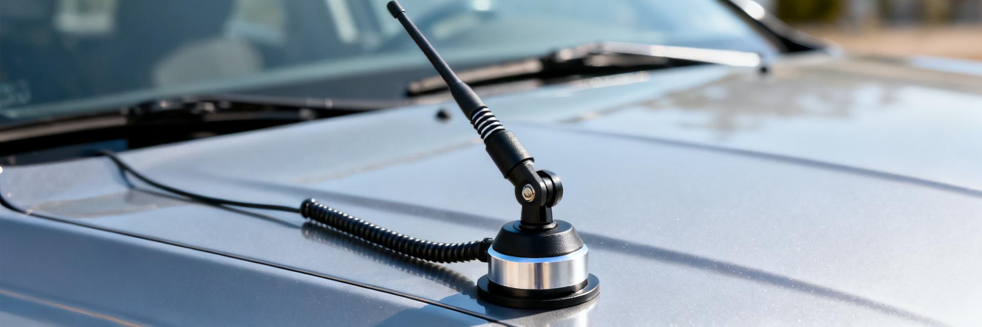
Lab and field test suites for mobile mag-mount antennas that cover ~880 MHz–2.17 GHz commonly report nominal gains near 3 dBi and VSWR figures under 2.5 across each band. This article uses those baselines to walk through performance expectations, common specs and test methods for a compact mag-mount solution, explaining measurement, installation, and troubleshooting steps for reliable mobile links. Product overview & design highlights (Background) What the PE51113-2 is and who it’s for This mobile mag-mount omnidirectional whip targets mid/high cellular and ISM bands, intended for temporary vehicle installs, site surveys, and rapid IoT gateway prototyping. The class trades ultimate range for portability and ease: quick deployment, low profile, and omnidirectional coverage make it suitable for telemetry, mobile data and temporary field operations where simplicity and repeatable RF behavior matter. Key design elements to call out The design pairs a flexible metal whip and ferrite-backed magnetic base sized for typical vehicle roofs or metal plates. Expected connector class is an N-type female/male interface on the cable end, with a 5–12 foot coax lead common in the category. The magnet assumes a moderate ground plane; materials and whip length set resonance and handling of wind and vibration. Full technical specs explained (Data analysis) Nominal Performance Snapshot Gain: ~3 dBi VSWR: Freq: 2.17 GHz Electrical/RF specs to document Core specs include dual bands roughly 880–965 MHz and 1.71–2.17 GHz, nominal gain near 3 dBi, 50 Ω impedance and target VSWR under 2.5. Power handling is modest for mobile use. These specs matter because gain affects link margin, VSWR indicates matching and transmitter stress, and impedance ensures compatibility with typical radio transceivers and feedlines. Mechanical & environmental specs Mechanical specs to note: overall height (typical whip length ~10–16 inches), cable type and length, connector gender, and qualitative magnet holding force suitable for vehicle speeds. Temperature and humidity ratings are moderate; installers must consider roof clearance, wind load on the whip and vibration resilience when planning permanent or semi-permanent mounts. Lab and field performance tests (Data-driven) Recommended test methodology & setup A repeatable test matrix includes a VSWR sweep with a calibrated VNA, gain/pattern checks in an anechoic or reflected-field environment, and throughput/coverage trials using representative radios measuring RSSI and packet error rates. Required gear: VNA, RSSI-capable transceiver, calibrated cables, and a standardized metal ground plane to simulate vehicle rooftop conditions for consistent comparison versus baseline. Typical test results and how to interpret them Expected outcomes: VSWR curves showing dip regions in both bands with peaks under 2.5, near-omnidirectional azimuth patterns on a vehicle roof and modest elevation lobing. Compare measured gain to published ~3 dBi; log delta vs. baseline, plot VSWR across frequency, and use thresholds (VSWR Installation & mounting best practices (Methods) Pre-install checks & mounting tips Confirm a solid metal ground plane or use a dedicated mounting plate for optimal coupling. Place the magnet near the vehicle centerline, clean surfaces to remove debris, and inspect magnet seating to prevent sliding. Maintain clearance from moving parts and fuel lines; keep separation from other antennas to limit pattern distortion and intermodulation in multi-antenna installs. Cable routing, connectors, and grounding Route coax with gentle bends, secure with clips to avoid chafing and stress at the connector, and torque connectors to recommended values. Use silicone or approved boots for waterproofing. Add ferrite chokes near the radio to suppress common-mode currents and ensure a good chassis ground to reduce RF noise and potential interference with vehicle electronics. Comparative use cases & pairing guidance (Case study) Use-case scenarios that fit this antenna Typical deployments include mobile voice/data, remote telemetry and temporary gateway setups where quick install and omnidirectional coverage are priorities. Expect trade-offs: compact mag-mount convenience versus lower gain and reduced long-range performance compared to higher-gain or directional antennas, making it ideal for cellular aggregation and short- to medium-range telemetry. Matching radios, power levels, and antennas alternatives Match transmit power to regulatory limits and link budget; modest transmit power pairs well with this antenna’s ~3 dBi gain for urban and suburban ranges. For extended coverage choose higher-gain or directional antennas and consider permanent mast mounts. Antenna selection should weigh portability, required range, and installation permanence. Buying, maintenance & troubleshooting checklist (Actionable) Pre-purchase checklist (what to confirm) Frequency coverage matches the intended band plan. Verify connector type and cable length. Review declared gain, VSWR and mechanical specs. Confirm mounting footprint and magnet assumptions. Common faults and quick fixes VSWR spikes after installation often come from loose connectors, damaged coax or poor magnet seating—re-torque connectors and inspect the cable. Intermittent loss can indicate ground plane issues or chafed coax; reseat the magnet and reroute. Run a quick VNA sweep to isolate the fault before requesting replacement if the antenna fails bench thresholds. Key summary Performance: The mobile mag-mount delivers ~3 dBi nominal gain and VSWR Installation: A clean, central metallic ground plane and secured cable routing preserve patterns; use ferrites for noise reduction. Application: Best for temporary deployments; consider permanent mast mounts for long-range fixed needs. Common questions & answers Does the PE51113-2 require a large ground plane? Mag-mounts perform best with a conductive ground plane; a vehicle roof or a dedicated metal plate approximates performance conditions used in specs. Small plates reduce low-frequency efficiency and can raise VSWR. How should one verify VSWR and gain after mounting? A quick verification uses a VNA sweep to capture VSWR across both bands and an RSSI-based throughput test with a representative radio for field gain validation. When is replacement preferable to troubleshooting? If bench VSWR and continuity checks show sharp mismatches or open/shorted elements after basic fixes, replacement is appropriate. Summary The PE51113-2 provides a compact, mobile-friendly dual-band magnetic antenna solution with trade-offs between portability and range. Verify the published specs, run VSWR and coverage tests after mounting, and follow the pre-purchase and installation checklist to maximize field performance. Compile a short test sheet of VSWR, gain and coverage to decide if a mag-mount fits permanent or temporary deployment needs.