• AD8236ARMZ-R7 Datasheet Breakdown: Key Specs & Metrics

    Core Thesis: The AD8236ARMZ-R7 positions itself as an ultra-low-power instrumentation amplifier with headline numbers that drive design decisions: quiescent current in the 40 µA class and a single-supply span down to 1.8 V (Datasheet Table 1). Design Evidence: Those figures make it highly attractive for battery-powered and wearable front ends. Low quiescent current directly reduces standby drain in always-on sensor nodes and widens battery life projections for intermittent-sampling designs. ⌖ Background & At-a-Glance Overview A concise background lets engineers triage the part quickly. The device is a micropower instrumentation amplifier intended for low-power sensor front ends and portable data-acquisition systems (Datasheet Overview). Knowing the class and intended use narrows checks for supply conditions, bandwidth, and gain ranges early in component selection. Typical Applications The AD8236ARMZ-R7 is designed for low-amplitude signal conditioning in: Wearable electronic devices Battery-powered industrial sensors Medical instrumentation front-ends Quick Decision Box Supply Range 1.8 V – 5.5 V Quiescent Current ~40 µA Output Type Rail-to-Rail Key Benefit Micropower Front-end Electrical Performance Deep-Dive Understanding how power and rails affect system behavior is essential. Designers should convert quiescent current into battery life estimates (e.g., 40 µA on a 100 mAh cell yields theoretical standby durations) and account for active-mode consumption in system budgets. Operational Range Visualization Supply Voltage (V) 1.8V to 5.5V Quiescent Current (µA) Max 40µA (Typ) Power & Output Swing Supply headroom and output swing define usable dynamic range. The amplifier supports single-supply operation and offers rail-to-rail behavior. Caution: Expect limited headroom near rails under heavier loads; validate worst-case temperature to confirm required output swing. Precision Metrics Accuracy is governed by CMRR, input bias, and offset. Rule of thumb: effective differential error ≈ common-mode voltage / 10^(CMRR(dB)/20). Use the datasheet values to compute system-level common-mode error based on your chosen gain. Environmental & Reliability Metrics Parameter Significance Design Action Temp Drift Limits long-term accuracy at low frequencies. Include calibration intervals for ppm-level stability. Packaging Affects thermal margin and PCB footprint. Allow thermal margin in copper for small packages. ESD/Reliability Robustness against transients. Add protection at the input for field survival. Design and Integration Guide Gain Setting & Components The amplifier uses an external resistor (Rg) to set closed-loop gain. For a target output: Gain = Vout_target / Vin_expected Choose resistor tolerances and low-drift parts to preserve DC accuracy. Pair gain selection with input filtering to limit bandwidth and noise. PCB Layout Best Practices ✓ Local decoupling within millimeters of supply pins. ✓ Route inputs as guarded differential pairs. ✓ Use star ground topology to minimize noise. Bench Validation & Test Conditions Reproducing datasheet numbers requires matching exact test conditions (gain, supply, load, temperature). Any deviation in source impedance or measurement bandwidth will result in lagging performance numbers. Pro-Tip: Isolate causes of deviation by simplifying the test—disconnect filters, lower source impedance, and validate each block (supply, grounding, input source) individually. Recommended Setup Use a precision source, low-leakage fixtures, and a spectrum analyzer. Account for source impedance when measuring input bias and noise to ensure the environment doesn't dominate the measurement. Selection Checklist & Action Items When to use this part Ultra-low quiescent current is the priority. Rail-to-rail output is required for wide dynamic range. Single-supply operation (as low as 1.8V). Modest bandwidth needs. Release to Prototype Verify pinout and footprint. Add discrete decoupling and input protection. Label test pads for offset/noise debug. Commit to BOM after power budget check. Summary Micropower Leader: Delivers ultra-low standby drain (~40 µA) for battery-centric designs. Accuracy Matters: Validate rail-to-rail behavior and CMRR under your specific gain and load; bench tests must mirror datasheet conditions. Integration Focus: Follow tight layout rules and use recommended decoupling to ensure prototype performance meets expectations. Frequently Asked Questions How do I verify AD8236ARMZ-R7 quiescent current on the bench? + Measure quiescent current with a precision current meter in series with the supply while the inputs are tied to their common-mode voltage and the output is unloaded. Ensure you match the datasheet's gain, load, and temperature conditions to reproduce the stated ~40 µA measurement. What datasheet specs most affect low-level signal accuracy? + CMRR, input bias, offset, and noise are the dominant specs. Check the datasheet tables for typical and maximum values and consider how source impedance and gain amplify these error sources in your system-level error budget. Which test points should I include for initial prototype validation? + Include supply, ground, differential inputs, amplifier output, and a test point after any input filter. Also add a shielded guard plane connection for low-bias measurements and pads to inject known test signals for gain, offset, and noise characterization.
  • TLE6209R Performance Report: Motor Current & Thermal

    Core Point The TLE6209R shows a practical continuous current envelope that guides motor control limits. Evidence suggests continuous capability near 5–6 A with short peaks to 6–7 A under ideal conditions. Engineering Focus Focuses on measurable motor current behavior and thermal response. Bench-style checks emphasize RMS under PWM, inrush peaks, and junction temperature delta (ΔT). Background: Why the TLE6209R matters for motor control Key device parameters to track Key parameters determine current limits and heating. It is essential to track continuous/peak output current, supply range, RDS(on), thermal shutdown threshold, recommended junction temperature, and short-circuit protections. These define safe operating boundaries in system contexts. Typical operating scenarios and load profiles Motor use cases create distinct current and thermal patterns. Startup draws high inrush, stall produces extended peaks, and PWM duty cycles set RMS. Mapping these profiles predicts when derating or active cooling is needed to avoid thermal trips. Motor Current Analysis: steady-state, transient, and peak behavior Current Capacity Visualization (Amperes) Continuous Operating Range 5A - 6A Short-term Peak Limit 7A Steady-state and RMS current characterization RMS current under PWM is the dominant contributor to continuous heating. By measuring IRMS vs duty cycle and computing power as I2·RDS(on) plus switching losses, designers can accurately quantify PCB cooling requirements. Transients, startup and stall currents Short-duration peaks stress the thermal budget. Capturing peak amplitude with a high-speed scope lets designers determine if Over-Current (OC) events will trigger and whether hardware or firmware limiting is required. Thermal Performance: junction temp, thermal resistance, and cooling needs Metric Description Application RthJA / RthJC Thermal resistance metrics to compute ΔT = P × Rth. Predicts safe junction temperature (Tj) vs ambient. Tj Limit Device thermal trip point and recommended operating temp. Defines operational limits and throttling policies. Derating Curves Current vs Ambient temperature boundaries. Provides clear limits for sustained duty cycles. Test Methodology & Measurement Setup • Bench Setup: Requires a programmable DC supply, electronic load, high-speed oscilloscope, and thermocouples. • Protocols: Standardized runs at 25/60/85°C, PWM frequency sweeps, and long-duration soak tests. Design & Thermal Management Best Practice: Maximize copper area beneath the package, add thermal vias to internal planes, and implement firmware soft-start or adaptive PWM throttling to prevent runaway heating. Summary Continuous and peak current ranges define design margins. Prioritize PCB thermal area and firmware control to keep junction rise within the recommended envelope for the TLE6209R. 1 Verify continuous current and peak behavior under representative loads and ambient temperatures. 2 Compute power dissipation from IRMS and RDS(on) to size PCB copper and cooling strategies. 3 Combine hardware (vias, airflow) and firmware (soft-start) to avoid thermal shutdown. Frequently Asked Questions How should I measure continuous current for accurate motor driver assessments? Use a low-inductance shunt or calibrated current probe with a high-speed oscilloscope to capture steady and transient events. Record long-duration I(t) to compute IRMS under intended PWM duty cycles and log temperature so power dissipation and thermal response can be correlated to junction rise. What thermal metrics are most critical when evaluating motor driver performance? Report power dissipation, RthJA/RthJC-based ΔT, steady-state junction temperature, and thermal time constant. These metrics show whether steady dissipation will exceed safe junction temperatures in the expected ambient. Which firmware strategies most effectively prevent thermal trips in motor applications? Implement soft-start to limit inrush, adaptive PWM duty limiting based on ADC-read temperature and current, and scheduled cool-down intervals during sustained high-load periods. These measures reduce cumulative energy into the package.
  • JW5357MSOTB Datasheet Deep Dive: Specs, Bench Data

    Point: Engineers favor compact synchronous buck converters for tight point-of-load regulation where input range, continuous output current, and efficiency matter. Evidence: Typical design targets are multi-volt input windows, sustained 2–4 A outputs, and efficiency above 85% at mid-load. Explanation: This article uses datasheet values and measured bench data to translate those metrics into actionable design choices for a compact synchronous buck, with emphasis on layout, thermal strategy, and validation methodology. Overview: JW5357MSOTB at a Glance Key Specifications Summary Point: The part presents a compact power stage aimed at small point-of-load tasks. Evidence: Datasheet values list a multi-volt VIN window, integrated MOSFETs, and a specified max continuous current. Parameter Typical Value (Datasheet) Input Voltage Range 4.5–18 V Max Continuous Output Current Up to 3 A (thermally limited) Switching Frequency 1.2 MHz (nominal) Package / Pins MSOP-like with exposed pad Internal MOSFET Topology Synchronous N-channel high/low side Recommended Output Caps MLCCs with low-ESR, plus optional bulk Thermal Warning: The compact package imposes thermal constraints. Expect full-current operation only with aggressive PCB thermal strategy—exposed pad soldering, thermal vias, and adequate copper are must-haves for sustained loads. Datasheet Walkthrough: Electrical Characteristics and Pinout Pinout & Recommended Footprint Correct interpretation of pinout (FB, SW, VIN, VOUT, GND, EN) and exposed pad is critical. Route VIN and input caps close to the VIN pin, place VOUT sense adjacent to the VOUT pin, and stitch the exposed pad with a grid of thermal vias. Operating Conditions & Limits Design with derating—operate VIN well below absolute max (18V), limit continuous current to allow a 10–20°C margin to thermal shutdown, and validate over expected ambient extremes on the bench. Power-Stage and Thermal Behavior Efficiency Visualization (Datasheet Baseline) Mid-load Efficiency (Target vs. Measured) 88% Efficiency Switching Architecture: Use on-resistance to estimate conduction loss (I²·Rds(on)) and combine gate charge with frequency to approximate switching losses. Thermal Resistance: Junction rise depends on PCB design. Calculate: Tj = Tambient + (Power_Loss × RθJA). Reduce RθJA with multiple thermal vias and generous copper pours. Bench Data and Performance Measurements Measurement Setup ✔ Kelvin sense for VOUT measurements. ✔ Input caps within millimeters of VIN pin. ✔ Log ambient temperatures with thermocouples. Key Performance Charts Essential plots include Efficiency vs. Load (for multiple VINs), Power Loss Breakdown, VOUT Ripple, and Transient Load Response. Compare measured curves to datasheet plots to identify layout issues. Reference Design Scenarios Scenario A: Mobile Battery-Fed Target VIN ~4.5–12 V, VOUT 3.3 V, Peak 2 A. Prioritize thermal vias under the exposed pad and use low-profile MLCCs for space efficiency. Scenario B: Industrial 12V Rail VIN 9–18 V, VOUT 5 V, Sustained 3 A. Use larger copper pours and additional input bulk capacitance for transient immunity. Key Summary 1 Understand datasheet limits: Treat absolute maximums as one-time events and use recommended operating conditions with margins. 2 Prioritize PCB thermal work: Exposed pad soldering and thermal via arrays control sustained current capability. 3 Measure methodically: Capture efficiency, ripple, and transient response under controlled ambient conditions. 4 Troubleshoot systematically: Isolate layout parasitics first before changing the power stage or topology. Frequently Asked Questions How do I verify JW5357MSOTB thermal limits on my board? + Point: Use controlled load steps and thermal imaging to validate dissipation. Evidence: Measure board temperature at steady-state and compute Tj using RθJA. Explanation: If junction approaches the limit, add more vias, copper, or reduce load to remain within safe margins. What bench data should I publish for efficiency claims? + Point: Publish standardized plots for transparency. Evidence: Provide efficiency vs. load at key VIN values and transient recovery. Explanation: Include full test conditions (VIN, VOUT, ambient) so results can be reproduced and deviations understood. Which layout mistakes most commonly degrade performance? + Point: Long VIN-to-SW loops and poor pad soldering are frequent culprits. Evidence: Loop inductance raises ringing; poor pad contact increases RθJA. Explanation: Keep input caps adjacent to VIN, minimize SW loop area, and ensure full exposed pad soldering with thermal vias.
  • MC34119G-S08-R Technical Report: Pinout, Specs & Tests

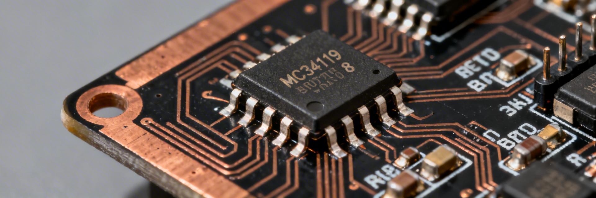
    Measured with a 3.3 V supply and an 8 Ω load, many low‑power audio amplifiers in this class deliver output power in the 200–500 mW range while drawing under 10 mA quiescent current. This technical report examines the MC34119G-S08-R — its verified electrical specs, test procedures, and troubleshooting guidance. Part Overview & Key Specifications Typical Use Cases The device is a low‑power single‑chip audio amplifier intended for small speakers and handsets. Typical applications include portable audio modules, telephone handsets, intercoms, and battery‑powered notification speakers. Performance metrics include a single‑supply operating range of 2.5–5.5 V and typical output power into 8 Ω on the order of a few hundred milliwatts. Quick Specs Summary Table Parameter Typical / Range Design Significance Supply Voltage (VCC) ≈ 2.5–5.5 V Determines available output swing and compatibility with system rails. Quiescent Current (Iq) ~5–10 mA Critical for battery life and standby power drain. Output Power @ 3.3V, 8Ω ~200–400 mW Optimized for small speakers and handset loudness. THD+N < 1–2% Ensures audio fidelity at rated output levels. SNR ~70–85 dB Defines the noise floor for quiet signals. Pinout & Functional Description Electrical Roles The pinout follows an SOP‑8 audio amplifier footprint. Typical pin‑level voltages feature VCC rail at system voltage, and inputs biased near VCC/2 for single‑ended operation. Outputs are centered at midrail DC. Always observe ESD precautions and use input clamping where signal swings may exceed rails. External Components Required decoupling: 0.1 µF ceramic within 5 mm of the VCC pin and a 4.7–10 µF bulk capacitor for low‑frequency stability. Use 0.1–1 µF input coupling capacitors. Add 33–100 Ω series resistors at inputs to damp HF ringing. Test Procedures & Bench Results Expected Performance Visualized Output Power @ 3.3V (mW) SNR Efficiency (dB) *Bench data based on 8 Ω resistive load at 1 kHz sine input. Methodology • Use a low‑noise DC source with 0.1 µF + 4.7 µF decoupling. • Drive with 1 kHz sine through known source impedance. • Monitor package temperature with defined ambient conditions. Interpretation Define pass/fail: power within ±20% of target, THD below specified threshold. Variance often stems from PCB thermal resistance and measurement bandwidth. Typical Application Circuits & Design Tips Reference Schematic Guidance: Provide a basic single‑supply driver: VCC decoupled 0.1 µF + 4.7 µF, input coupling cap 1 µF to IN+, IN− tied to bias network. For BTL devices, outputs drive 8 Ω without output capacitors. Use the control pin via a 100 kΩ resistor for soft transitions to reduce clicks. PCB Layout Checklist ✅ Solid ground plane ✅ Close VCC decoupling ✅ Short/Equal output traces ✅ Thermal vias under package Troubleshooting & Best Practices Common Failure Modes No Output: Check VCC and ground continuity.Distorted Audio: Verify supply decoupling.Excessive Heat: Measure thermal rise; improve copper pour. Production Checklist Perform BOM review for capacitor voltage ratings. Run layout peer reviews focused on thermal paths. Execute EMI pre‑compliance tests with ferrite filtering. Summary PINOUT Confirm VCC, GND, inputs, and MUTE/EN behavior; implement 0.1 µF decoupling to avoid DC offsets. SPECS Expect single‑supply operation (2.5–5.5 V) and quiescent current in the single‑digit mA range. TESTS Use 1 kHz sine and 8 Ω loads; set pass/fail criteria with ±20% power tolerance for pilot production. Frequently Asked Questions What is the recommended decoupling and input coupling for the amplifier? + Use a 0.1 µF ceramic close to the VCC pin and a 4.7–10 µF bulk capacitor within the power island to stabilize low‑frequency transients. For inputs, choose 0.1–1 µF coupling capacitors sized to the input impedance. How should I verify thermal performance on a prototype? + Measure ambient and package temperatures under continuous sine at near‑rated output for 15–30 minutes. If rise exceeds allowable values, increase copper area, add thermal vias, or reduce continuous power via duty cycling. What are the quick steps for MC34119G-S08-R troubleshooting? + Confirm VCC is stable, check mute/control pin logic, probe inputs for expected signal amplitude, and measure output DC offset. Test with a known resistive load to isolate the issue.
  • LM5050MKX-2 Datasheet Deep Dive: Critical Specs & Tests

    Strategic Insight: This article translates the LM5050MKX-2 datasheet into actionable checks and lab tests for system engineers. Key datasheet items determine system behavior: operating input range, quiescent current, transient tolerance, and documented test modes. Validation Goal: Move from passive reading to a prioritized verification plan. Confirm margins, MOSFET pairing, layout impact, and thermal behavior in a real-world board environment for US-market power systems. What the LM5050MKX-2 Does and Where It Fits Functional Overview The device functions as a high-side ideal-diode / OR-ing FET controller, commanding an external N-channel MOSFET so the board conducts when its rail is highest and blocks reverse conduction when not. Internally, it senses input and output nodes and drives the gate to minimize drop while protecting against transients and reverse current. At the system level, it replaces diode-based OR-ing to reduce loss and pairs with a chosen MOSFET to set conduction loss and transient robustness. Application Scenarios Common uses include redundant power shelves, hot-swap inputs, and battery OR-ing where low voltage drop and fast isolation matter. Compared to diode OR-ing, FET controllers reduce conduction loss but add layout complexity. Designers trade simplicity for efficiency: selecting a MOSFET with low RDS(on) lowers steady loss but increases gate charge, making gate-drive capability a critical design lever. Critical Electrical Specifications Supply Voltage & Transient Analysis The electrical front-end specs define allowed rail voltages, standby draw, and transient survival. For design margin, adopt at least 20% derating on the operating range. Operating Range (V) Safe Margin: 20% Derating Applied Quiescent Current (IQ) Efficiency Minimal Idle Loss Gate Driver & Charge Pump Gate-drive amplitude and timing specs determine achievable MOSFET VGS. Ensure VGS stays within limits during spikes, checking that rise/fall rates do not induce large di/dt voltage overshoot. Verify the charge pump maintains stable amplitude under load transients to ensure the MOSFET remains in the safe operating area. Thermal, Reliability & Mechanical Specs Category Critical Parameter Design Action Thermal θJA / Junction Temp Locate thermocouples at pins; run soak tests. Mechanical Footprint / Pad Size Keep gate traces short; place bypass caps close. Reliability Reflow Profile Verify profile to avoid tombstoning in production. Testing LM5050MKX-2: Bench Procedures Required Equipment ⚡ Two Programmable DC Supplies ⚡ High-Bandwidth Current Probe ⚡ Electronic Loads & ESR Meter ⚡ Thermal Camera / Thermocouples Functional Steps Build a test fixture with external MOSFET and input sense points. Capture IN/OUT voltage, gate waveforms, and load current. Define pass/fail thresholds like Vdrop under specified current and absence of reverse conduction. Save golden waveforms for design reviews. Interpreting Test Results: Troubleshooting FAQ What are typical failure modes in the lab? ▾ Common failures include excessive Vdrop, false shutdowns, and incomplete gate drive. Measurements often show voltage spikes or delayed gate response pointing to layout inductance, wrong MOSFET selection, or insufficient gate-drive margin. How do I debug measurement artifacts? ▾ Avoid artifacts by using differential probes for floating nodes and short ground leads on scope probes. Confirm probes do not load the gate. Use oscilloscope traces to correlate slow gate edges with high Qg or weak drive. What is the recommended debug checklist? ▾ 1. Verify supply rails and bypassing. 2. Examine layout for long gate or sense traces. 3. Swap MOSFETs to rule out part-specific issues. 4. Reproduce faults under controlled pulses with one variable change per run. Design & Integration Checklist for Production Component & Layout ✅ MOSFET VGS(max) margin of 20–30% ✅ RDS(on) optimized for expected current ✅ Local decoupling within millimeters of pins ✅ TVS protection sized for expected transients System Verification ✅ Functional boot & full load OR-ing ✅ Thermal soak at worst-case ambient ✅ Automated bench scripts for repeatability ✅ Peak Vdrop within go/no-go thresholds Executive Summary The LM5050MKX-2 provides high-side ideal-diode control; validate operating range, quiescent current, and transient tolerance before selecting external parts. Key lab checks include startup/dropout ramps, gate waveform captures, and thermal measurements to diagnose layout or MOSFET selection faults. Production readiness requires MOSFETs with VGS margins, strict adherence to footprint/bypass placement, and automated functional tests.
  • INA145 Datasheet: Key Specs & Measured Performance

    Data-driven bench comparisons for precision difference amplifiers often reveal measurable gaps between datasheet claims and real-world behavior—small percentage differences in offset, CMRR, or bandwidth can break high-accuracy signal chains. This article uses the INA145 datasheet as a reference to show which INA145 specs matter most and how measured performance typically compares in practice. Overview — What the INA145 is and Where it's Used Core Architecture & Functional Blocks Point: The INA145 is a programmable-gain difference amplifier built around a precision internal resistor network and external gain resistors. Evidence: The architecture places matched internal resistors in the signal path and relies on a single external resistor to set gain. Explanation: This topology reduces resistor-matching error and simplifies gain setting, lowering gain error and improving CMRR compared with discrete resistor implementations; however, input offset and output swing remain tied to internal amplifier stages and supply rails. Typical Application Spaces Point: Typical uses include sensor front ends, low-level differential signal conditioning, and precision data acquisition. Evidence: Designers commonly place the part where small offsets or common-mode voltages exist, such as bridge sensors or differential RTD amplifiers. Explanation: Common stressors are single-supply operation near rails, large common-mode voltages, and wide temperature swings; these conditions shift offset, reduce CMRR, and may expose bandwidth or output drive limits. INA145 Datasheet — Key Specifications to Watch Electrical Specs that Determine Performance Point: Extract the following INA145 specs to predict system behavior: supply range, quiescent current, input offset and drift, input bias current, CMRR, PSRR, gain range, bandwidth, slew rate, and output drive. Evidence: Each parameter on the datasheet is typically listed with test conditions—VCC, load and temperature—plus typical and maximum values. Explanation: For meaningful comparison, capture units (µV, dB, µA, kHz), test VCC (single vs dual), load (RL), and the temperature or “typical” vs “maximum” columns to separate expected versus worst-case behavior. Mechanical, Thermal, and Reliability Specs Point: Packaging, operating temperature, thermal resistance, and absolute maximum ratings constrain applications. Evidence: Datasheet thermal resistance and maximum junction or supply ratings determine power and ambient limits. Explanation: Pay attention to thermal derating and output current limits—higher ambient or sustained output drive can push junction temperature, increasing offset drift and potentially violating reliability thresholds in tight enclosures. INA145 Datasheet vs. Measured Performance Simple Test Schematic V+ ----+----[VCC]----+ | | IN+ ---+--||--Rin--+ | | |-- INA145 -- RS -- RL -- GND IN- ---+-----+ | | | GND ---+------------+ Gain set by Rgain from datasheet test point Test Setup & Measurement Methodology Point: Reproduce datasheet conditions to obtain comparable measured performance. Evidence: A recommended setup uses the same gain setting, supply rails, load, and ambient as the datasheet. Explanation: Use precision DC sources, low-noise signal generators, and a high-resolution DMM or ADC. Watch probe loading, source impedance, and ground loops. Measurement Results & Comparison Report Parameter Datasheet (typ/max) Measured Value % Difference Visual Deviation Input Offset 50 µV (typ) 85 µV +70% CMRR @ 50 Hz 100 dB (typ) 88 dB -12% Small-Signal BW 200 kHz (typ) 170 kHz -15% Noise (nV/√Hz) 8 nV/√Hz 9.6 nV/√Hz +20% Frequency Response Visualization (Relative) Gain Freq f0 (Cutoff) How to Test and Verify INA145 Specs on Your Bench Recommended Test Circuits Use simple, repeatable circuits for offset, gain error, CMRR, PSRR, bandwidth, and noise. Measure offset with shorted inputs and known gain; measure CMRR by applying equal common-mode voltage while injecting a differential signal. Choose 0.01% precision resistors and low-ESR bypass capacitors close to VCC pins. Measurement Tips Minimize setup contributions: use low-capacitance probes, four-wire Kelvin connections for low-level DC, and shielded cables. Verify instrument bandwidth exceeds part bandwidth, enable averaging for noise measurements, and use a measurement checklist for consistent grounding. Design & Selection Checklist ✓ Tradeoffs: Balance precision, speed, and power. Choose this family when matched-resistor precision and compact gain setting are priorities. ✓ Layout: Use short input traces, guard rings around high-impedance nodes, and star grounding to reduce errors. ✓ Optimization: Use tight resistor matching and thermal relief for stable operating temperature to address measured shortfalls. Key Summary The INA145 datasheet highlights key electrical parameters—offset, CMRR, PSRR, and bandwidth—that determine suitability for precision differential amplification. Measured performance often shows modest degradation versus datasheet typical values due to layout, temperature, and source impedance. Follow recommended test circuits: precision resistors, close decoupling, and low-impedance probes for repeatable comparisons. Use the provided comparison table to decide if the INA145UA meets your specific system tradeoffs. Common Questions and Answers How do I interpret INA145 datasheet offset versus measured performance? + Compare the datasheet “typical” and “maximum” columns under the same test conditions you apply. Measured offset will often sit above the typical value; if it approaches the datasheet maximum, investigate layout, temperature and input sourcing. Use Kelvin wiring and short traces to distinguish device drift from setup error. What are the best practices to verify INA145 specs for CMRR and PSRR? + Apply controlled common-mode voltage while injecting a small differential signal for CMRR; measure output change and calculate dB. For PSRR, inject a known ripple on VCC and measure output amplitude. Match datasheet gain and load, and ensure test source impedance is low. Can I trust the INA145 datasheet for bandwidth and noise in my design? + Datasheet values are a baseline measured under ideal conditions. Your measured bandwidth and noise may be degraded by layout, source impedance, and external filtering. Verify on-board with proper instrumentation and accept a practical tolerance band using the methodology in this article. How many times should I repeat measurements to confirm stability? + Perform at least three repeat runs across relevant ambient temperatures and supply variations, documenting mean and standard deviation. For noise and low-frequency CMRR, longer acquisitions with averaging yield more reliable statistical measures. Conclusion The INA145 datasheet identifies parameters critical to precision differential amplification, but measured performance can differ because of test conditions, layout, and external components. Use the test methodology, comparison framework, and checklist provided here to validate INA145 specs in your application and make confident selection decisions based on real-world requirements.
  • SD18-1880R8UUA1: How to Read SAW Duplexer Specs Quickly

    SD18-1880R8UUA1: How to Read SAW Duplexer Specs Quickly Many RF engineers and product designers waste time hunting through long datasheets when they only need a few critical numbers to choose a component. This guide gives a repeatable, time-saving workflow to extract the essentials from the SD18-1880R8UUA1 datasheet. The Core Objective Point: The goal is speed without losing accuracy. Evidence: Experienced RF teams use a short checklist to avoid costly re-spins and field failures. Explanation: By scanning a consistent set of specs in a fixed order, you reduce subjective decisions and accelerate the procurement and validation cycle. Quick Background: What a SAW Duplexer Does and Why SD18-1880R8UUA1 Matters Point: A SAW duplexer separates transmit and receive paths using bandpass filters inside a single package. Evidence: In practical systems, the duplexer must present low insertion loss in Tx/Rx passbands while providing high isolation between ports. Explanation: That balance preserves link budget on transmit and prevents receiver desensitization. Point: Fast datasheet triage saves time to market. Evidence: Teams that judge parts on the right handful of electrical and mechanical numbers typically discard mismatches in hours, not days. Explanation: The SD18-1880R8UUA1 sits in a mid‑band class where center frequency and passband shape determine map compatibility. At-a-Glance Spec Summary for SD18-1880R8UUA1 Key Electrical Specs (Priority Radar) Parameter Typical Value Range Visual Benchmark Insertion Loss (Tx/Rx) < 2.5 dB Isolation (Tx-Rx) > 45 dB Return Loss > 10 dB Note: Scan priority: Must-have (Frequency, IL, Isolation) → Important (BW, Return Loss) → Nice-to-have (Power, Package). Step-by-Step: How to Read Each Critical Spec Frequency, Bandwidth & Filter Shape + Point: Translate center frequency and passband edges into usable channel range. Evidence: Datasheets often list center frequency and −3 dB/−1 dB passband edges. Explanation: Compute usable channel range by applying guard-band margins (usually 0.5–1.0 dB safety margin). Always check the test reference conditions to ensure apples-to-apples comparisons. Insertion Loss, Isolation & Return Loss + Point: Interpret insertion loss impact on link budget and isolation impact on receiver blocking. Evidence: Insertion loss appears as Tx power required or Rx sensitivity penalty. Explanation: Isolation above ~30 dB is often required; treat insertion loss under ~2 dB as acceptable for most handsets. Check values at both center and band edges for worst-case scenarios. Mechanical & Environmental Quick Checks + Point: Verify package size, terminal count, and temperature range. Evidence: Mechanical mismatches cause PCB layout changes or assembly issues. Explanation: Note which tolerances in the datasheet will drive layout updates and thermal derating for your specific application. Real-World Matching: Apply SD18-1880R8UUA1 to Your RF Design Handset Design ✔ High Power Handling ✔ Minimal Tx Insertion Loss ✔ Steep Selectivity IoT Nodes ✔ Ultra-Compact Footprint ✔ Low-Loss Receive Path ✔ Battery Life Optimization Quick Action Checklist & Troubleshooting Hardware Verification Confirm footprint/pinout compatibility. Measure S21 for Tx/Rx insertion loss. Measure isolation with fixture de-embedding. Next Steps if Borderline Evaluate matching/tuning networks. Request tighter test data from vendor. Prototype with conservative margins. Summary Point: Use a repeatable quick-read flow: background → at-a-glance specs → interpret key numbers → match to use-case → test. Evidence: Applying this flow to SD18-1880R8UUA1 cuts review time and reduces risk of field surprises. Explanation: The SD18-1880R8UUA1 should be judged primarily on center frequency alignment, insertion loss, and isolation; treat mechanical constraints and power handling as gating factors and always verify raw numbers against the official datasheet before final selection.
  • W25Q64JVSSIQ Datasheet — Complete SOIC‑8 Specs & Pinout

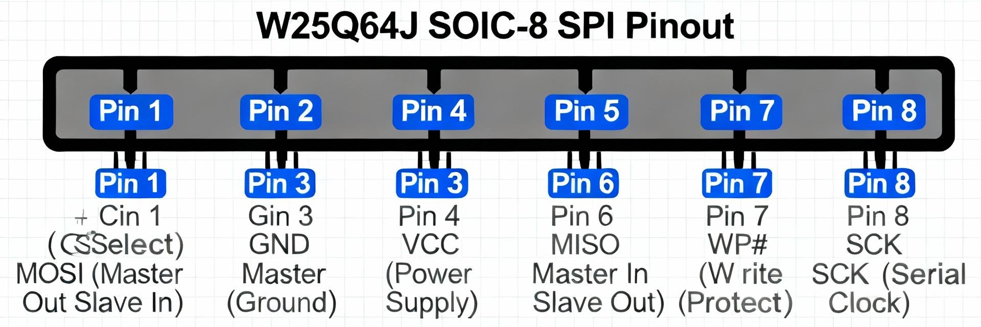
    Core Identification: The W25Q64JVSSIQ is a high-performance 64M‑bit serial NOR flash memory designed specifically for code storage and efficient data logging. It provides a reliable 64 Mbit (8 M x 8) density, operating within a 2.7–3.6 V supply range, and supports high-speed SPI throughput up to 133 MHz in a compact SOIC‑8 (5.30 mm body) form factor. Quick Overview: Device Identity, Primary Specs & Typical Uses Key Specs at a Glance Density 64 Megabit Max Clock Speed 133 MHz Voltage Range 2.7V – 3.6V Nominal: 3.3V Operation Evidence: The W25Q64JVSSIQ features an erase organization of 128 blocks and 2,048 sectors, supporting standard SPI, Dual, and Quad modes. Explanation: These architectural choices allow designers to balance power consumption (active read current ~25 mA) and thermal management within an operating window of −40 °C to +85 °C. Typical Applications The device's small footprint and high-speed interface make it an ideal choice for firmware storage, configuration parameter logging, boot ROM, and embedded data logging. Its low pin count reduces PCB complexity and overall Bill of Materials (BOM) costs. Complete Electrical & Memory Characteristics Power, Current & Thermal Limits Parameter Specification Range Recommended Usage Supply Voltage (VCC) 2.7 V to 3.6 V 3.3 V Nominal Active Read Current Up to 25 mA Decoupling: 0.1 µF + 1 µF Standby Current µA range Critical for battery devices Memory Layout & Endurance The memory architecture is built for granularity: 256-byte pages, 4 KB sectors, and 32/64 KB blocks. Typical endurance exceeds 100,000 cycles per sector, with data retention lasting multiple decades. SOIC-8 Package & Pinout Configuration SOIC-8 Top View (Standard Pinout) /CS [1]DO [2]WP# [3]GND [4] [8] VCC[7] HOLD#[6] CLK[5] DI Full Pin Functions Pin 1: /CS (Chip Select) - MCU Chip Select active low Pin 2: DO (MISO) - Data Output (I/O1) Pin 3: WP# (Write Protect) - Hardware write protection Pin 4: GND - Common Ground Pin 5: DI (MOSI) - Data Input (I/O0) Pin 6: CLK - Serial Clock Input Pin 7: HOLD# - Pause serial communication Pin 8: VCC - 2.7V to 3.6V Power Supply Integration Guide: SPI Commands & Read/Write Flows // Essential SPI Opcodes for W25Q64JVSSIQ 0x03 - Read Data | 0x06 - Write Enable 0x20 - Sector Erase (4KB) | 0x02 - Page Program 0x05 - Read Status Register | 0x9F - JEDEC ID Methodology: The standard transaction pattern requires setting CS Low, sending the Opcode, followed by Address/Data, and concluding with CS High. Software must poll the WIP (Work In Progress) bit via the Status Register after any write or erase operation. Testing, Troubleshooting & Best Practices Lab Debug Checklist Verify VCC/GND rails with an oscilloscope. Confirm /CS toggling and SPI mode (0 or 3). Read JEDEC ID (0x9F) as the first functional test. Check pull-up resistors on WP# and HOLD#. Reliability Tips Implement wear-leveling to extend flash life. Use CRC verification for firmware updates. Keep SPI traces short and impedance-matched. Ensure monotonic VCC rise during power-up. Summary of Design Considerations ✔ Compact Specs 64 Mbit capacity, 3.3V nominal, 133 MHz. Essential for high-speed boot sequences. ✔ Pinout Precision SOIC-8 body width 0.209". Pin 8 bypass capacitor is mandatory for noise reduction. ✔ Endurance Planning 100k+ cycles; leverage 4KB sectors for efficient OTA and data management. Frequently Asked Questions ▶ Where can I verify opcodes from the W25Q64JVSSIQ datasheet? Consult the official datasheet PDF provided by the chip vendor to confirm exact opcode bytes, dummy cycles, and timing. This is mandatory before firmware deployment as revisions can affect specific commands. ▶ What is the best practice to wire the SOIC‑8 to a 3.3 V MCU? Tie VCC to 3.3 V, place a 0.1 µF bypass capacitor within 2 mm of Pin 8, and connect WP#/HOLD# to VCC via 10 kΩ pull‑ups. Use short traces for MOSI/MISO/CLK to ensure signal integrity at high speeds. ▶ How do I minimize wear and accidental erases? Use sector-sized write buffering and log compaction. Protect critical boot regions with software locks or the hardware WP# pin. Always implement dual-bank update patterns to prevent bricking during power failures.
  • STM32F413VGT6 Datasheet Deep Dive: Pinout & Core Specs

    Advanced Pinout Analysis & Core Specifications for Professional Layout Planning The STM32F413VGT6 is a high-performance ARM® Cortex®-M4 class microcontroller integrated with DSP instructions and a dedicated Floating Point Unit (FPU). Encapsulated in a 100-pin LQFP package, it balances robust flash/SRAM capacity with high-speed processing. This guide extracts mission-critical data for designers to streamline schematic capture and PCB layout. Quick Overview: STM32F413VGT6 at a Glance Optimized for compute-intensive embedded tasks such as digital audio processing, industrial motor control, and high-speed signal handling. It delivers deterministic real-time performance with significant on-chip memory for medium-to-large firmware footprints. Key Identity and Use Cases This Cortex-M4 DSP/FPU-capable MCU is the backbone for real-time applications requiring high core throughput and expanded peripheral sets without moving to high-power application processors. One-Line Spec Snapshot Parameter Typical Value (Datasheet) Visual Scale CPU Architecture ARM Cortex-M4 with DSP/FPU Max Clock Speed Up to 100 MHz Flash Memory 1 MB SRAM Capacity 320 KB Package LQFP-100 14 x 14 mm Datasheet Core Specs Deep-Dive: CPU, Memory, and Performance Core metrics are found in the datasheet's processor feature section. Key focus areas should include the ART Accelerator™, flash access latencies across clock domains, and recommended wait states to estimate MIPS/workload capacity. Core & Performance Metrics Includes single-precision FPU and DSP instructions. ART/cache behavior ensures zero-wait state execution from Flash up to the maximum frequency. Memory Map Details Precise mapping of boot regions, option bytes, and SRAM partitions. Essential for DMA buffer placement and OTA region sizing. Pinout & Package Breakdown Package Overview and Pin Mapping Strategic grouping of power pins and high-speed IO clusters is vital for floorplanning. The LQFP-100 layout requires careful attention to decoupling capacitor proximity and analog/digital domain isolation. ✔ Group VDD/VSS pins for low-impedance paths. ✔ Route high-speed peripherals (SPI/SDIO) with matched lengths. ✔ Maintain contiguous ground planes under the MCU. Critical Pins Identification Always verify the following pin groups in the datasheet Pinout Table: VDD / VSS NRST OSC_IN / OUT BOOT0 SWDIO / SWCLK VBAT Peripherals, I/O and Electrical Characteristics The STM32F413VGT6 features a rich array of peripherals including UART, SPI, I2C, ADC/DAC, and specialized DFSDM (Digital Filter for Sigma-Delta Modulators). DMA controllers are crucial for managing high-bandwidth signaling without CPU intervention. Signaling Constraints Consult Alternate Function (AF) tables early. Prioritize time-critical interfaces to avoid pin-mux conflicts between high-speed timers and communication ports. Electrical & Thermal Limits Respect per-pin source/sink current limits. The datasheet specifies absolute maximum ratings vs. recommended operating conditions—ensure safety margins for industrial environments. Real-World PCB Integration Case Study Example: Minimal-Power Sensor Gateway A gateway using 3.3V rail, 32.768 kHz RTC crystal, and UART/SPI communication. Key layout goals: single regulator headroom, precise decoupling (0.1µF + 10µF), and crystal placement within 5mm of pins. Common Pitfalls Missing decoupling on secondary VDD pins. Improper thermal relief for the 100-pin LQFP. Inadequate pull-up/down resistors for BOOT configuration. Practical Design & Debug Checklist Pre-Silicon Checklist (Schematic & BOM) Verify VREF+ and VDDA isolation for ADC accuracy. Check NRST reset network timing constants. Include test points for SWDIO, SWCLK, and UART TX/RX. Placeholder footprints for ferrite beads on power rails. First-Power-Up & Bring-Up Checklist Confirm 3.3V steady-state voltage and sequencing. Validate crystal oscillation and frequency accuracy. Execute "LED Blink" and UART "Heartbeat" firmware. Verify Flash programming via SWD/JTAG. STM32 Summary The datasheet is the authoritative reference for electrical limits and layout recommendations. Treat figures and tables as primary sources to ensure the reliable integration of the STM32F413VGT6. Extract core, clock, and memory info to seed BOM. Map power/ground and reserve debug headers early. Follow stepwise bring-up to isolate hardware vs. software issues. Frequently Asked Questions What are the essential power and reset pins to verify during bring-up? ▾ Verify all VDD and VSS pins per the datasheet’s pinout. Ensure dedicated VDD_IO or VREF pins are powered correctly. NRST should be held high with an internal or external pull-up, and decoupling capacitors must be placed as close to the power pins as possible to minimize EMI. How should I read the memory map to place bootloader and application partitions? ▾ Consult the Memory Map figure to identify Flash sectors (Sectors 0-11 typically). Allocate the bootloader to the earliest sectors, reserve middle sectors for application code, and use the upper sectors for non-volatile data storage. RAM should be partitioned for stack, heap, and DMA-friendly buffers. Which electrical characteristics are critical to check for IO and thermal safety? ▾ Prioritize the Absolute Maximum Ratings for supply voltage and I/O input levels. Check the Total Current into VDD to ensure your power supply can handle peak core and peripheral usage. Calculate thermal dissipation based on the Package Thermal Resistance (θJA) to ensure the junction temperature stays within the specified operating range.
  • MTFC8GAKAJCN-4M-IT eMMC 8GB Real-World Performance

    Core Insight: Datasheet specs list sequential read ~190 MB/s and sequential write ~22 MB/s for the MTFC8GAKAJCN-4M-IT, but in-system results vary markedly. Evidence: Engineers commonly see a spread from near-datasheet read rates down to lower sustained write throughput depending on workload, bus mode, and thermal limits. This article presents reproducible benchmark approaches, observed ranges, and practical tuning steps for evaluating eMMC 8GB performance in embedded products. What the MTFC8GAKAJCN-4M-IT eMMC 8GB is and where it fits Key Specs at a Glance Typical datasheet callouts for this 8 GB (64 Gbit) module cite eMMC 5.x interface, sequential read ≈190 MB/s and sequential write ≈22 MB/s, 3.3 V supply range, and industrial operating temperature options. Capacity, interface version, and rated speeds set host-controller and power budgets. Target Applications Common targets include IoT gateways, industrial controllers, and consumer devices requiring a compact boot+data store. 8GB eMMC is chosen when cost, predictable latency for boot, and low PCB area outweigh the need for higher write endurance. Real-world I/O Benchmarks: Sequential and Random Performance Throughput Visualization (MB/s) Sequential Read (Datasheet)190 MB/s Sequential Read (Observed Range)160 - 190 MB/s Sequential Write (Datasheet)22 MB/s Performance Metric Datasheet Spec Observed Results Sequential Read ~190 MB/s 160–190 MB/s Sequential Write ~22 MB/s 10–40 MB/s (Workload dependent) 4K Random Read Not typically listed Hundreds–Thousands IOPS Thermal and Endurance Power scales with activity and bus mode. Active read/write currents typically rise with throughput. Estimate field life by combining expected daily writes, overprovisioning, and wear-leveling characteristics. Monitor active vs idle energy per MB. MLC-class NAND shows finite P/E cycles. High temps directly reduce data retention. System Integration eMMC settings and layout materially influence boot times. Enabling HS bus modes and using a dedicated boot partition can cut cold-boot latency significantly. Verify HS200/HS400 mode negotiation. Optimize filesystem (f2fs or ext4 with tuned journaling). Tune driver buffers for throughput balance. Bench Test Checklist and Optimization Playbook Reproducible Suite Run sequential large-block throughput, 4K random Q1 and QD8 tests using fio. Capture median and p95 latency traces to set pass/fail thresholds. Practical Tweaks Reserve spare area for overprovisioning, improve thermal conduction paths, and smooth write patterns to increase steady-state lifespan. Summary ✔ Datasheet vs Observed: MTFC8GAKAJCN-4M-IT lists ~190 MB/s read and ~22 MB/s write; expect actual reads of 160–190 MB/s and writes of 10–40 MB/s based on thermal constraints. ✔ Impactful Checks: Focus on 4K random benchmarks, thermal traces during sustained load, and filesystem tuning to reduce write amplification. ✔ Prioritized Plan: Run fio suite, validate HS mode, and iterate over overprovisioning to balance performance and endurance. Frequently Asked Questions What real-world performance should I expect from eMMC 8GB in an embedded product? + Expect sequential reads near datasheet peaks under ideal host conditions but sustained writes that vary widely; plan for sequential write rates anywhere from roughly 10–40 MB/s and 4K random IOPS in the hundreds to low thousands depending on queue depth and controller behavior. How should I benchmark the MTFC8GAKAJCN-4M-IT to validate product requirements? + Use a reproducible fio-based suite: large-block sequential read/write, 4K random read/write at QD1 and QD8, and a sustained mixed workload for 10–30 minutes while logging temperature and power; compare median and p95 latencies against system targets. What are the highest-leverage optimizations to improve eMMC performance? + Enable verified high-speed bus modes, reserve spare area (overprovision), tune filesystem mount options to reduce small synchronous writes, and improve thermal paths; implement changes incrementally and document impact on throughput and endurance.