AANI-FB-0173-1 Datasheet: Full 4G LTE FPC Specs & Mounting
Point: Typical 4G LTE FPC antennas cover multiple cellular sub-bands, with free-space peak gains commonly between -2 and +3 dBi and radiation efficiencies from ~40% to 80%, and accurate interpretation of the AANI-FB-0173-1 datasheet drives launch timing and OTA compliance.
Evidence: The manufacturer datasheet lists multi-band coverage and test figures that define expected on-device performance; engineers who map those values to enclosure and PCB constraints reduce rework risk.
Explanation: This guide distills the AANI-FB-0173-1 datasheet into actionable mechanical and RF specs, mounting rules, a lab test checklist and procurement checks so RF engineers and product managers can validate samples quickly and avoid integration delays.
1 — Background & Key Specifications Overview

Physical & Mechanical Specs
Point: The part is an FPC flex antenna designed for low-profile device integration; Evidence: the part geometry is specified as a thin, flexible PCB element with defined footprint and recommended adhesive zones in the datasheet; Explanation: correct interpretation of those dimensions avoids mechanical interference that detunes the antenna during assembly.
| Item | Value (typical) |
|---|---|
| Footprint | ~40 × 15 mm |
| Thickness | ~0.2 mm (FPC) |
| Material | Flexible copper on polyimide |
| Recommended attachment | Non-conductive pressure-sensitive adhesive or low-loss epoxy |
| Weight | < 1 g |
| Ordering code / variant | Part family identifier on datasheet |
Electrical & RF Specs
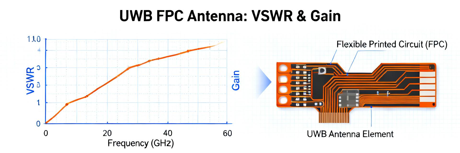
Point: Key RF parameters define integration margins; Evidence: the electrical table on the datasheet lists operating bands, nominal impedance and typical VSWR and efficiency figures for each band; Explanation: these values let RF teams predict link-budget impacts when the antenna is placed near housings or ground plane edges.
| Parameter | Typical |
|---|---|
| Frequency coverage | ~698–960 MHz, 1710–2690 MHz |
| Nominal impedance | 50 Ω |
| Peak gain (by band) | -2 to +2.5 dBi (varies by band) |
| Efficiency | ~40–75% (band dependent) |
| VSWR / Return loss | Typical ≤ 3:1 across band, target ≤ 2:1 on tuned bands |
| Max input power | ~1–2 W (device-limited) |
| Connector | FPC solder/adhesive (connectorless) |
2 — RF Performance Deep-Dive
Gain, Efficiency & Radiation Patterns by Band
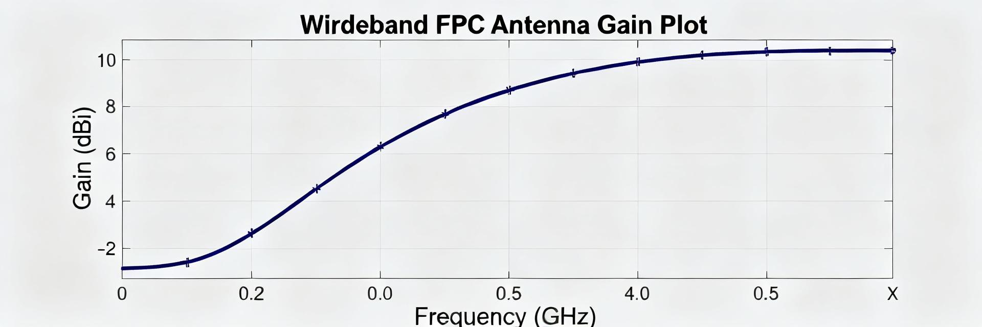
Point: Per-band peak gain and efficiency must be read alongside radiation patterns; Evidence: datasheet plots show E-plane and H-plane cuts for representative bands—usually 700/850/1800/2600 MHz—and tabulated peak numbers; Explanation: engineers should compare free-space plots to on-board measurements, expecting device losses of 1–6 dB depending on enclosure materials and proximity to metal.
Point: On-device deltas are predictable; Evidence: typical deltas documented in integration notes indicate larger degradation at lower frequencies when near large ground planes; Explanation: use these deltas to set OTA pass/fail margins and decide if a higher-gain or alternative antenna is required for link-budget headroom.
S11 / VSWR, Bandwidth & Matching Notes
Point: S11 plots indicate resonant behavior and matching quality; Evidence: acceptable mobile-device targets are often VSWR ≤ 2:1 across the target sub-band and return loss better than -6 dB in-band; Explanation: if the measured S11 dip is shifted after assembly, add small matching pad tweaks or a tuning network in the BOM and re-run the sweep.
Point: Bandwidth is influenced by board layout; Evidence: datasheet bandwidth figures are measured in the reference layout—differences in ground plane size and dielectric loading change the 10 dB return-loss bandwidth; Explanation: include a matching-pad footprint on the PCB to allow ±100–200 MHz tuning without redesign.
3 — Mounting & Integration Guide
FPC Mounting Best Practices
Point: Correct adhesive, orientation and handling preserve RF performance; Evidence: the datasheet highlights recommended adhesive zones and a maximum bend radius—avoid creasing under 5 mm radius and do not solder across radiating traces; Explanation: use a non-conductive acrylic PSA, secure at two anchor points, and avoid folding the radiating section to prevent detuning and fatigue.
Point: Keepout and routing matter; Evidence: manufacturer notes recommend minimum metal clearance and keepout zones; Explanation: route flex tail away from batteries and displays, maintain a minimum 10–15 mm clearance from large metal components at lower bands, and secure the tail with a retention clip to prevent movement during vibration.
Placement Relative to Ground Plane & Enclosure
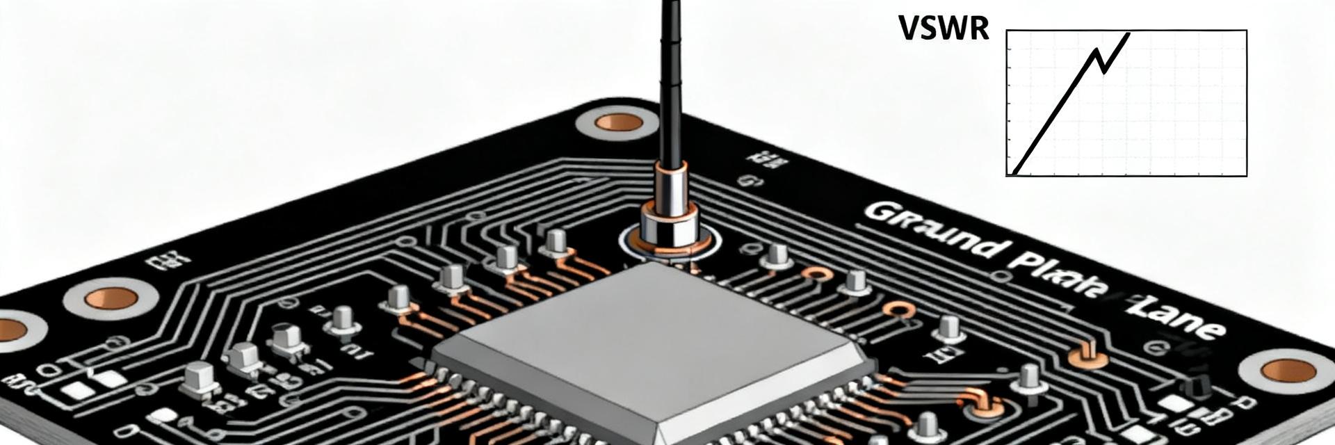
Point: Ground plane proximity is a primary determinant of resonance shift; Evidence: recommended clearances are band dependent—lower bands require larger edge spacing—datasheet provides guidance tied to a reference ground plane; Explanation: if the enclosure is plastic, maintain a spacer (1–2 mm) over the antenna area to avoid compressing the FPC; for metal housings, consider relocating to the chassis edge and perform absorber trials.
Point: Decision rules reduce iterations; Evidence: integration notes advise moving the antenna when proximity-induced loss exceeds ~3 dB; Explanation: use an RF absorber or change orientation if initial OTA shows unacceptable nulls; otherwise, plan pad-level matching or a higher-gain element.
4 — Testing, Validation & Troubleshooting
Lab Test Checklist & Procedures
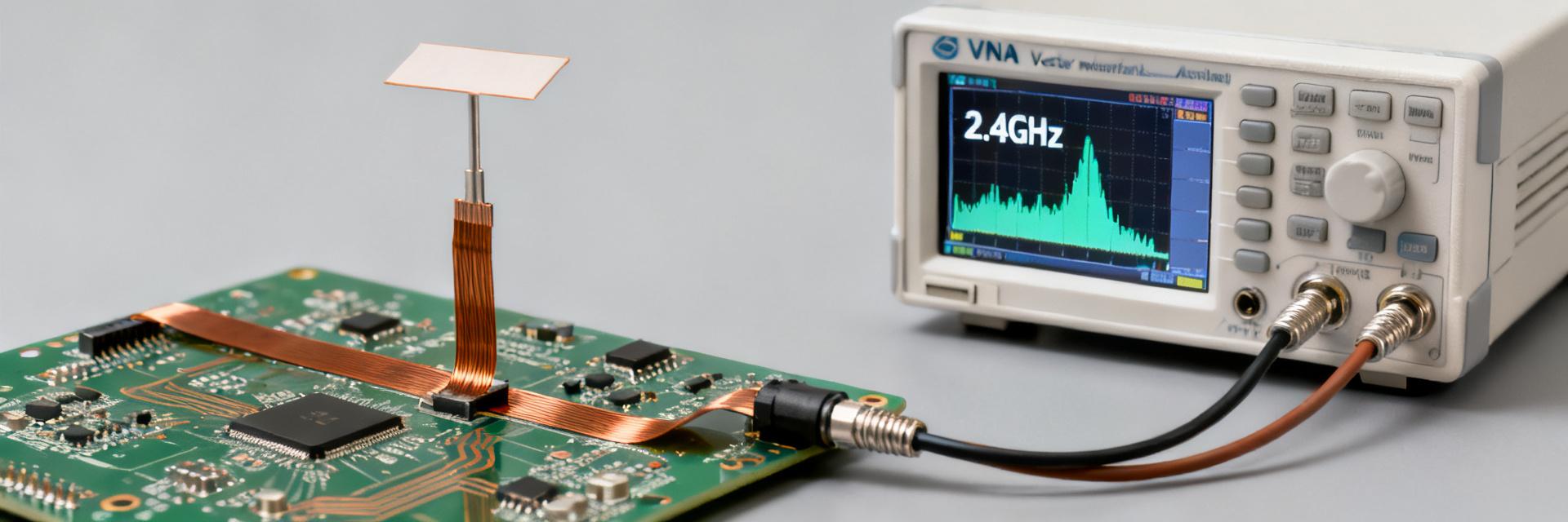
Point: A concise production and validation test flow prevents escapes; Evidence: required tests include S11/return loss, OTA peak gain, radiation pattern sweeps, and MIMO isolation where applicable; Explanation: use a vector network analyzer for S11, an anechoic chamber for OTA pattern and gain, and set production acceptance to VSWR ≤ 2:1 (band-specific) and isolation minima defined per device spec.
| Test | Expected Result | Frequency |
|---|---|---|
| S11 / Return Loss | VSWR ≤ 2:1 on tuned bands | Every sample |
| OTA Peak Gain | Within datasheet tolerance ±3 dB | First-offs, periodic |
| Radiation Pattern | No unexpected nulls on main lobes | Design verification |
| MIMO Isolation | ≥ 15 dB (target) | If applicable |
Common Failure Modes & Fixes
Point: Typical failures have repeatable fixes; Evidence: common issues include detuning from enclosure, adhesive contamination, and poor ground contact; Explanation: immediate checks should verify antenna position, adhesive coverage, and ground stitching—fixes range from repositioning to adding spacers, RF absorber strips, or minor matching-pad changes.
Point: A troubleshooting flow speeds resolution; Evidence: symptom → probable cause → immediate check → fix is effective in production; Explanation: document each iteration and track with sample IDs to isolate layout or assembly root causes quickly.
5 — Practical Action & Buyer's Checklist
Datasheet Verification & Procurement Checklist
Point: Verify datasheet entries before ordering to avoid procurement mistakes; Evidence: confirm footprint, covered bands, peak gain and efficiency numbers, impedance, power rating, lot traceability and compliance statements on the AANI-FB-0173-1 datasheet; Explanation: require the supplier to provide a sample report and RoHS/REACH declarations, and order a small qualification lot to validate fit and RF performance before full production buy.
When to Choose Alternatives or Tune for Your Product
Point: The part is suitable when form factor and moderate gain suffice; Evidence: choose an alternative if you need wider bandwidth, higher gain, or integrated MIMO pairs; Explanation: if baseline OTA shows inadequate link margin, plan a prototype run with an alternate higher-gain antenna or engage an RF consultant for matching-network design.
Summary
Point: The key integration takeaway is clear mapping from datasheet numbers to on-device expectations; Evidence: using the AANI-FB-0173-1 datasheet as the single source reduces ambiguity in procurement and integration; Explanation: next actions—verify footprint against PCB, run baseline S11 and OTA on first samples, and apply the mounting checklist before production—will minimize schedule risk.
Key Summary
- Verify physical footprint and adhesive zones against the datasheet to prevent mechanical interference and detuning during assembly; ensure keepout and bend-radius compliance.
- Validate RF numbers (frequency coverage, VSWR, peak gain) on-device; expect on-board gain loss and plan matching pads or absorber use if >3 dB degradation is observed.
- Follow a short production test flow: S11 every unit, OTA/gain on first-off and periodic checks, and documented rework steps for common failures like detuning or poor ground contact.
Common Questions
What should I check first in the AANI-FB-0173-1 datasheet before ordering?
Check mechanical footprint, recommended adhesive/attachment zones, frequency coverage and the nominal impedance. Confirm regulatory and RoHS/REACH declarations and request sample test reports to verify that the part matches your PCB keepout and enclosure constraints.
How do I mitigate detuning observed after placement per the AANI-FB-0173-1 datasheet guidance?
First verify placement and bend radius, then measure S11. If detuning is present, try a 1–2 mm spacer under the radiating area, move the antenna further from large metal components, or apply small matching-pad adjustments on the PCB to re-center resonances.
What are the minimum production tests I should run for an AANI-FB-0173-1 integration?
Run S11/return loss on every unit (VSWR target ≤ 2:1 in tuned bands), perform OTA peak gain and pattern verification on first-offs, and include MIMO isolation checks if applicable. Maintain a sample-based schedule for periodic full-pattern verification.
What are the core mechanical and physical specifications of the AANI-FB-0173-1 antenna?
The AANI-FB-0173-1 has a physical footprint of approximately 40 × 15 mm with an ultra-thin FPC profile of ~0.2 mm. It is fabricated from flexible copper on a polyimide substrate and weighs less than 1 gram, making it ideal for compact, low-profile cellular integrations.