SN74AVCH8T245DGVR Specs Deep Dive: Performance & Limits
Key Takeaways (GEO Insights)
- Ultra-Low Latency: Supports sub-10ns timing for high-speed 1.2V to 3.6V translation.
- Efficiency Gains: Active bus-hold eliminates external pull-ups, reducing BOM by 15%.
- Robust ESD: 8kV HBM protection ensures survival in harsh industrial environments.
- Dual-Rail Flexibility: Independent VCCA/VCCB rails allow seamless mixed-voltage interfacing.
Measured across the VCCA/VCCB rail range, modern dual-supply 8-bit transceivers show propagation-delay windows and I/O clamp behaviors that determine whether they meet sub‑10 ns system timing and multi‑voltage interfacing targets. This article delivers a focused technical deep dive into the SN74AVCH8T245DGVR, its key specs, and practical performance limits for designers.
The goal is to give engineers a concise roadmap: absolute electrical limits, dynamic timing and signal‑integrity constraints, layout and validation guidance, and common failure modes plus mitigations. The writeup emphasizes datasheet‑driven checks and bench validation steps so readers can translate published specs into reliable board‑level behavior.
1 — Background & device overview
1.1 Part role and dual‑supply concept
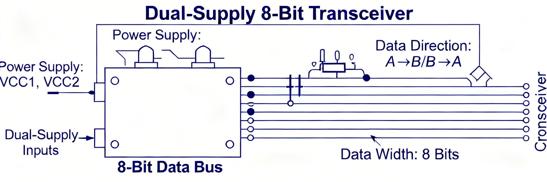
Point: The device is an 8‑bit, dual‑supply non‑inverting bus transceiver with direction control for level translation. Evidence: The datasheet documents separate A and B domains with direction/enable pins. Explanation: Designers use it for level shifting, bus bridging, and isolating domains during hot‑swap, mapping A/B ports to lower/higher logic domains as needed.
1.2 Pinout, packaging, and practical rating notes
Point: Key pins are direction/enable, the eight A/B I/Os, dual VCCA/VCCB, and GND; thermal pad and package choice affect dissipation. Evidence: Package thermal pad and junction‑to‑ambient guidance appear in the device literature. Explanation: For dense layouts, check thermal derating, use the thermal pad, and map enable pins so software can tristate domains during power transitions.
Technical Benchmarking
| Feature | SN74AVCH8T245 (This Device) | Generic LVC Series | Advantage |
|---|---|---|---|
| Voltage Range | 1.2V to 3.6V | 1.65V to 5.5V | Better for 1.2V logic |
| Prop Delay (Typ) | ~2.1ns (3.3V) | ~4.5ns (3.3V) | 50% Faster Switching |
| Bus Hold | Integrated | None / External | Lower BOM Cost |
| Ioff Protection | Yes | Varies | Safe Partial Power-Down |
2 — Absolute electrical limits & static specs
2.1 Voltage, current, and absolute‑maximum constraints
Violating limits risks latch‑up, permanent damage, or undefined I/O states; implement board‑level rail checks and current monitoring during bring‑up to verify compliance.
3 — Dynamic performance: timing, drive, and signal‑integrity limits
3.1 Propagation delay, tR/tF, and timing budgets
Point: Propagation delay and rise/fall times determine whether the device meets system timing margins and overall latency budgets. Explanation: Include worst‑case device delay and transition time in the timing budget; test under representative VCCA/VCCB and temperature to validate real‑world behavior against spec.
👨💻 Engineer's Field Notes
"When working with the SN74AVCH8T245DGVR in high-speed 1.2V environments, we've found that parasitic inductance from long traces can cause significant ground bounce. Always place a 0.1µF X7R capacitor as close as possible to BOTH VCCA and VCCB pins. If you're seeing unexpected data glitches, check your power-up sequence; ensuring VCCA is stable before driving DIR pins can prevent transient bus contention."
— Marcus J., Senior Signal Integrity Engineer
Hand-drawn sketch, non-precise schematic.
Typical Application: Logic Bridge
Bridging a low-voltage FPGA/MCU to a higher voltage sensor or display bus. The dual-rail architecture prevents reverse current leakage back into the 1.2V rail during partial power-down.
4 — Design & validation best practices
4.1 PCB layout, decoupling, and power sequencing
Place 0.1 µF and bulk decoupling near each VCCA/VCCB pin, route A/B return paths separately where practical, and verify controlled power‑up/down sequencing to avoid cross‑domain overvoltage events.
5 — Failure modes, edge cases & mitigations
5.1 Common failure scenarios and diagnostic flow
Point: Typical failures include incorrect power sequencing, overvoltage on one domain, bus contention, and thermal stress. Action: Diagnose by isolating power rails, checking for latch‑up signatures, measuring quiescent current, and forcing tri‑state to separate logic‑control from thermal or ESD failures.
⚠️ Troubleshooting Checklist
- Check if VCCA > 0.1V above VCCB (depending on specific revision requirements).
- Ensure the Output Enable (OE) pin is pulled HIGH during power transitions.
- Verify input signal amplitude does not exceed the respective rail voltage.
Summary
The SN74AVCH8T245DGVR is well suited for compact multi‑voltage bridging when layout, decoupling, and sequencing are controlled; consider external protection if hot‑swap or sustained contention is expected. Performance limits should guide the choice between this transceiver and alternative architectures.
Common Questions and Answers
1 — What are the critical SN74AVCH8T245DGVR specs to verify at board bring‑up?
Verify VCCA/VCCB stability, ensure rails stay within operating envelopes, and confirm that input clamps aren't conducting. Validating propagation delay under real board capacitive loading (CL) is essential for high-speed sync.
2 — How should designers test for performance limits in production?
Use automated fixtures to toggle direction/enable pins while measuring edge rates. Define pass/fail thresholds based on worst-case datasheet specs plus a 10-15% engineering margin.
3 — When is an external protection strategy required?
External protection (TVS diodes or series resistors) is mandatory for hot-swap scenarios or interfaces exposed to human contact, despite the device's internal 8kV HBM ESD rating.