


Helping you save cost and time.

Provide reliable packaging for your goods.

Quick and reliable delivery to save time.

Excellent after-sales service.
New Product Launch
More +

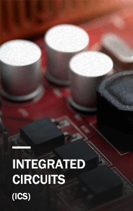
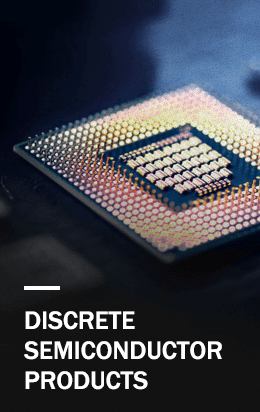
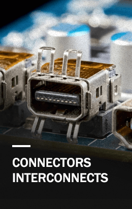
Hot Selling Parts


Blog
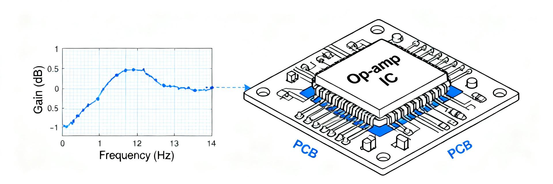
NL0333DCAE1S Op Amp Performance Report: Key Metrics Unpacked
Precision, low‑power amplifiers define the performance envelope for portable instrumentation. This report snapshots measured categories engineers prioritize—noise, gain‑bandwidth, slew rate and offset…
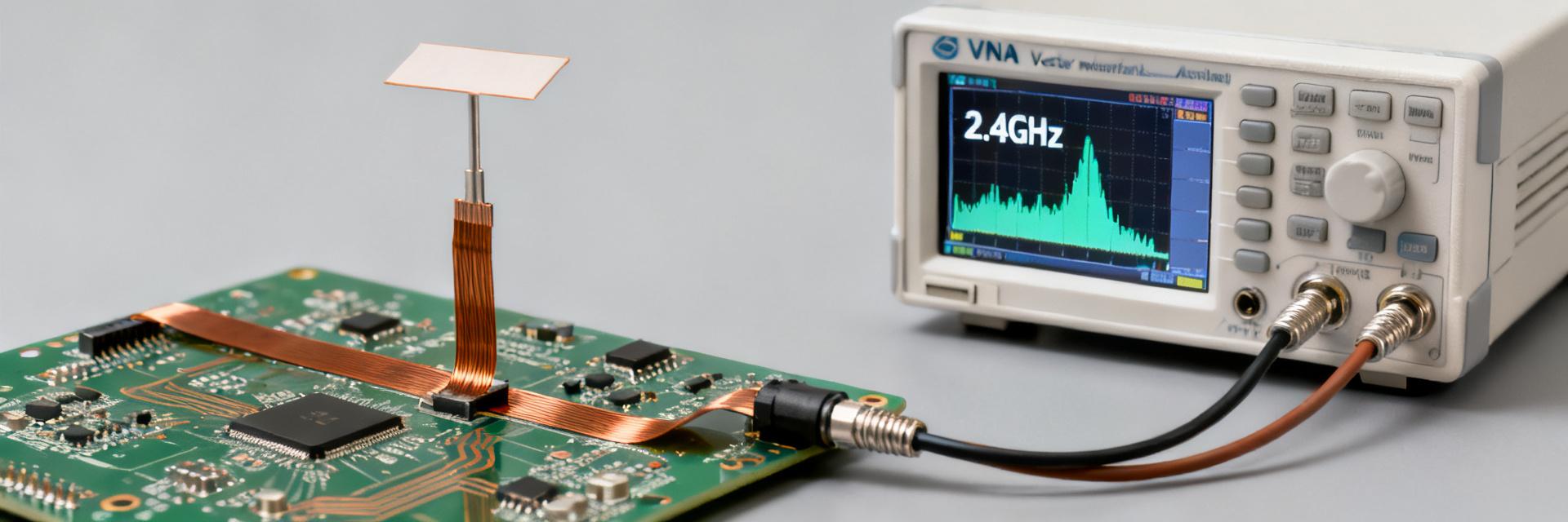
AANI-FB-0154-1 Performance Report: Measured 2.4GHz Specs
This report presents lab-measured 2.4 GHz RF performance for the AANI-FB-0154-1, highlighting measured VSWR band edges, peak gain and efficiency trends and comparing them to published targets. Measure…
Full-band FPC GNSS Antenna: Performance Report & Specs
2026-06-28 14:48:16
AANI-FB-0176-1 FPC Antenna: Measured Performance Report
2026-06-26 10:23:22
AANI-FB-0178-1 Antenna Report: Gain, VSWR & Efficiency
2026-06-21 10:16:53
AANI-FB-0032-1 Performance Report: Gain, SWR, Pattern
2026-06-17 12:00:18
AANI-FB-0174-1 FPC Antenna: Performance Report & Stats
2026-06-07 10:22:21
Read more